
A circuit no longer has to begin as a rigid green board on a factory bench. Conductive Ink Printing gives engineers, startups, and product teams a way to place working traces on plastic film, paper, textiles, glass, and molded parts without sending every early idea through the old board-making path. That matters in the United States because medical wearables, smart packaging, auto interiors, and defense sensors all keep asking the same question: can the circuit fit the shape of the product instead of forcing the product to fit the circuit? The answer is sometimes yes, and that “sometimes” is where the market gets interesting. For readers tracking electronics, hardware startups, and American manufacturing shifts, emerging electronics manufacturing coverage now belongs in the same conversation as chip design and battery supply chains. Printed electronics already support direct patterning of functional materials onto flexible and conventional surfaces, while flexible hybrid electronics mixes printed layers with semiconductor parts when raw silicon performance is still needed.
Conductive Ink Printing Is Moving Circuits Onto Surfaces
The best way to understand this shift is to stop thinking of a circuit as a separate object. On a printed sensor label, a heated car seat panel, or a disposable medical patch, the circuit can become part of the surface itself. That does not make old circuit boards obsolete. It makes them less lonely. For many products, the future is not board versus print. It is board plus print, placed where each one makes sense.
Why flat boards are not always the right answer
A standard printed circuit board is strong, repeatable, and trusted. It also wants a flat home. That becomes awkward when the product is curved, thin, soft, or meant to bend with a person’s body. A rigid board inside a skin patch is like a book cover sewn into a T-shirt. It can work, but you feel it.
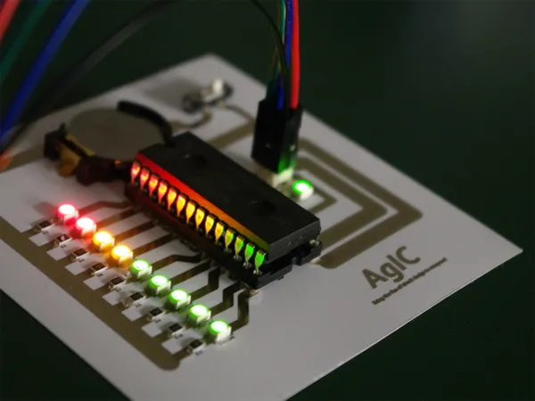
Printed electronics solves a different problem. It allows traces, antennas, electrodes, and simple sensors to sit on flexible substrates such as PET film, textiles, paper, or thin polymer sheets. Industry and research sources describe printed electronics as a way to make circuits and components through print processes rather than conventional board workflows, often using conductive inks on flexible materials.
The non-obvious part is that the printed layer is not always cheaper at first. Early runs may cost more because ink choice, drying, curing, registration, and testing still need care. The payoff comes when the shape, weight, assembly time, or user comfort improves enough to matter.
A bike helmet gives a plain example. You could hide a small board inside the shell for a crash sensor, but routing wires across a curved liner adds bulk and weak points. A printed sensor path on a thin film can follow the curve, then meet a small electronics island where the chip and battery sit. The circuit is not showing off. It is staying out of the way.
Where the printed layer earns its keep
Think about a smart package that confirms whether medicine stayed within a safe temperature range during shipping. A thick board and wired sensor would be overbuilt. A thin printed trace, a small chip, and a low-profile antenna can do the job while keeping the package close to normal.
The same logic fits auto interiors. A dashboard panel can carry touch controls, lighting traces, or heating elements under the surface. In-mold electronics and printed conductors can reduce parts, connectors, and hand assembly when the design is ready for volume. Some suppliers already describe silver inks as useful for three-dimensional formability and direct over-molding in this kind of work.
That is why smart device manufacturing trends should not be treated as a chip-only topic. The chip still matters, but the surface around it is getting smarter. The quiet win is not a sci-fi gadget. It is fewer screws, fewer wires, fewer hard edges, and fewer places for a small product to fail.
The strange part is that some printed traces are valuable even when they are not the main circuit. A printed shield, heater, touch area, or antenna can remove one awkward subassembly from a product. That is enough. In hardware, one removed connector can save more pain than one added feature.
The Materials Decide Whether The Idea Leaves The Lab
A printed circuit lives or dies by the ink and the surface beneath it. The printer gets the attention because it is easy to picture. The chemistry does the harder work. If the ink spreads too far, the line gets sloppy. If it does not stick, the circuit flakes off. If it needs too much heat, the plastic underneath may warp before the trace becomes useful.
Silver, copper, carbon, and the trade nobody escapes
Silver inks conduct well and have a long record in printed electronics. Copper costs less, but it can oxidize, which makes processing harder. Graphene, carbon nanotube, and carbon-based inks bring flexibility and material savings, though they may not match silver for every low-resistance job. NextFlex lists silver, copper, graphene, and highly doped carbon-based inks among passive conductor material sets used in flexible hybrid electronics.
There is no perfect ink. That is the point many product teams miss. A wearable sensor may accept more resistance if it survives bending and skin contact. An antenna may need a cleaner conductive path. A heater may care about controlled resistance rather than the lowest possible resistance.
A small American hardware team building a patch-style muscle monitor would not choose ink the way a company building a printed defroster grid would. Same broad field. Different pain. The serious work begins when the electrical target, bend radius, surface energy, cure temperature, and assembly plan are placed on the same table.
Ink handling also decides whether a process feels factory-ready. Shelf life, viscosity drift, nozzle clogging, and particle settling sound like small shop-floor annoyances. They are not small when a missed line breaks a sensor strip after packaging. A material that prints slower but behaves the same on Friday afternoon as it did Monday morning may be the better business choice.
Sintering sounds boring until it breaks the product
Many metallic inks do not conduct well the moment they land. They often need curing or sintering so the particles form better contact. That step sounds like a back-room detail until the product uses a low-cost plastic film that cannot take much heat.
This is why low-temperature processing matters. DOE material on roll-to-roll processing calls out challenges such as low-temperature work on bendable, stretchable, and foldable substrates, along with high-speed registration for multilayer devices. NextFlex has also noted that older nanoparticle silver inks may need sintering temperatures of 150°C and above, while newer reactive particle-free silver inks aim to improve inkjet performance and reliability.
Here is the counterintuitive lesson: the print step may be the easiest part to show and the least forgiving part to sell. A demo video can print a line in seconds. A factory has to print that line thousands of times, keep it narrow, dry it safely, attach components, test it, ship it, and still have it work after heat, moisture, bending, and time.
That is why engineering teams should test the ugly cases early. Fold the sample near the connector. Leave it in a hot car. Rub the surface. Add a cleaning wipe. The weak point often appears at the border between the printed trace and the hard component, not in the long clean line that looked perfect under a camera.
Printed Circuits Change Product Design Before They Change Factories
Printed layers do not only change how an item is made. They change what a designer dares to draw. Once circuitry can sit on a curved panel or a fabric strip, product teams stop hiding electronics in boxes and start treating them as part of the skin of the product. That shift is subtle, but it changes the first sketch.
Wearables become thinner when the circuit stops fighting the body
Most wearables still have a hard center. The band bends, the case does not. Printed layers can move some sensing and connection work into the flexible parts, leaving the chip and battery in the smallest hard area possible. That can make a patch feel less like a gadget and more like a bandage.
Healthcare is a strong fit because disposable or semi-disposable devices often need thin electrodes, short signal paths, and comfort. Printed medical electrodes, flexible sensors, and diagnostic patches can benefit from electronic circuits made close to the surface that touches the body. Companies serving printed electronics already point to medical electrodes, membrane switches, capacitive touch films, antennas, and e-textiles as common application areas.
The catch is trust. A hospital buyer does not care that a circuit was printed if the readings drift after sweat, motion, or storage. For medical use, the printed layer has to survive real life, not only a lab bench.
A home recovery patch for a knee patient shows the difference. The patient may bend, sleep, shower nearby, and forget the patch is there. If the printed electrode lifts at the edge, the data becomes noisy and the nurse loses confidence. Comfort gets the product worn. Reliability gets the data believed.
Smart packaging and labels need cheap intelligence, not tiny computers
A printed smart label is not trying to be a smartphone. It may only need an antenna, a sensor trace, or a tamper path. That modest job is what makes printed electronics practical. The product can gain one useful signal without carrying the cost and weight of a full electronics module.
For a U.S. grocery chain, that could mean cold-chain labels for seafood or vaccines. For a warehouse, it could mean a package that flags rough handling. For a retailer, it could mean shelf tags or anti-counterfeit marks that are thin enough to disappear into normal packaging.
This is where the old manufacturing mindset can get in the way. Engineers love more features. Printed labels win when they do less and do it cheaply. The best printed circuit in packaging may be the one customers never notice, because it hides inside the buying, shipping, or safety step that already exists.
Batteryless ideas fit this mindset well. A printed antenna tied to a small RFID or NFC chip can wake only when a reader comes near. That keeps the label thin and reduces parts. It also forces discipline. The circuit has to answer one job: identify, sense, prove, or warn.
The Manufacturing Promise Is Real, But It Has Limits
Printed electronics often gets described as a cleaner, simpler path because it adds material where needed instead of cutting copper away. That is true in spirit, but it should not be sold like a magic shortcut. Manufacturing still needs process control, inspection, materials handling, design rules, and trained operators. The promise is strongest when the product needs thin, large-area, flexible, or shaped circuitry.
Additive manufacturing reduces waste only when the process is controlled
Additive manufacturing can lower waste because the conductive material is placed in a pattern instead of removed from a larger sheet. That can be valuable when silver is involved, since wasted material is not cheap. It can also shorten some process flows by reducing etching, masking, or separate wiring steps.
Still, a bad print wastes ink, time, and substrate. A misaligned multilayer print can ruin the whole part. NIST-linked work on printed electronics infrastructure pointed to the interaction between ink and flexible substrates as a major performance challenge, especially because flow, adhesion, wetting, and batch variation can affect results.
So the greener story has a condition attached. Printing can cut waste when the line is tuned. Before that, it can create a different kind of scrap. Serious buyers should ask about yield, test method, repair plan, and end-of-life handling before they accept any smooth sustainability pitch.
Inspection also changes. A board shop can rely on decades of known checks, while printed layers may need optical scans, resistance maps, peel tests, bend tests, and moisture exposure. That adds work, but it also gives better feedback. When a line fails, the cause may point to screen wear, ink age, surface treatment, or oven behavior.
American factories may win in niches before they win at scale
The United States does not need to own every printed circuit job to benefit. The first wins may come in areas where speed, security, customization, or local engineering support matters more than the lowest unit cost. Defense sensors, medical patches, aerospace interiors, auto prototypes, and industrial monitoring are better targets than throwaway gadgets with razor-thin margins.
NextFlex defines flexible hybrid electronics as the intersection of printed and additively manufactured electronics with semiconductor devices, which fits this niche-first path. It lets manufacturers keep proven chips while printing the surrounding connections, antennas, or sensor layers where shape and weight matter.
That is a healthier way to read the field. Do not ask when printed circuits will replace boards. Ask where a board was never a good fit. That question leads to better products, cleaner pilots, and fewer claims that collapse during scale-up. For more background reading, the NIST report on printed electronics infrastructure needs is worth saving, especially for its focus on materials, measurement, and production gaps.
There is also a workforce angle. Printing a circuit asks for people who understand inks, presses, electronics, inspection, and assembly. That blend fits parts of the American industrial base that already know coating, converting, labeling, textiles, or medical device production. The advantage may come from shops that learn electronics, not only electronics firms that learn printing.
Short-run work may be the bridge. A regional converter in Ohio or New York does not need to beat Asia on every sensor label. It can help a medical or industrial customer tune a design, prove a process, and protect sensitive know-how close to the engineering team. That kind of local iteration is not glamorous. It is how new manufacturing habits stick.
Conclusion
The next wave of electronics will not arrive as one dramatic break from the factory floor. It will show up in smaller ways: a thinner medical patch, a smarter label, a curved control surface, a lighter sensor, a product that no longer needs a nest of wires to do a simple job. Conductive Ink Printing matters because it gives circuits permission to follow the product’s shape. Still, the winning teams will be the ones that respect the dull details: ink choice, curing, adhesion, inspection, and failure testing. That is where the promise becomes a product. For U.S. companies, the strongest opening is not chasing every low-cost board replacement. It is building printed layers into the places where comfort, shape, speed, and assembly savings carry real value. Pair this with future electronics design ideas, and the opportunity becomes clearer. Start with the surface, define the job, test the weak points early, and let the circuit earn its place.
Frequently Asked Questions
How does printed electronics differ from a traditional circuit board?
Printed electronics places conductive traces or functional layers onto a surface through print processes. A traditional board usually uses copper traces on a rigid or semi-rigid base. Printed designs work best when the product needs thin, flexible, lightweight, or shaped circuitry.
Is conductive ink safe for wearable devices?
It can be safe when the full material stack is designed and tested for skin contact, sweat, bending, and cleaning. The ink alone is not the whole answer. The substrate, coating, adhesive, battery, and regulatory path all matter for wearable products.
What materials can printed circuits be made on?
Common surfaces include PET film, polyimide, paper, textiles, glass, and molded plastics. The right choice depends on heat tolerance, bending needs, cost, moisture exposure, and how the finished part will be assembled or used.
Can printed electronics replace all circuit boards?
No. High-density computing, power electronics, and many complex devices still need standard boards and advanced chips. Printed layers are better for sensors, antennas, heaters, simple interconnects, touch controls, labels, and products where shape matters more than dense processing.
Why are silver inks used so often?
Silver conducts well and has a long track record in printed traces. It is also costly, so engineers may use copper or carbon-based options when the product can accept different electrical behavior, processing steps, or durability tradeoffs.
What is the biggest problem with printed circuits?
Reliability is often the hard part. A printed line may look fine at first, then fail after bending, heat, moisture, abrasion, or poor adhesion. Good testing has to copy the real environment, not only measure the fresh print.
Are printed circuits useful for small startups?
Yes, especially for prototypes, wearables, smart labels, and products that need unusual shapes. Startups should avoid assuming print will lower cost on day one. The better early reason is speed, form freedom, and fast design learning.
What industries in the USA could use this first?
Medical devices, automotive interiors, defense sensing, aerospace, logistics, packaging, and industrial monitoring are strong candidates. These fields often value thin form factors, local engineering help, faster pilots, and custom sensor layouts more than mass-market consumer goods.